Its figures speak for themselves: 50MHz operation, sub-200ps dead-time, and 120V/ns slew rate at the switching node.
The child of National Chiao Tung University and Realtek Semiconductor, both in Taiwan, the IC is GaN-on-silicon, combining a half-bridge with analogue and digital control circuits.
As there is no ‘p-type’ GaN transistor, cmos-like complementary circuits are impossible on a GaN IC.
Instead, in this case, analogue and digital blocks are built from actively-controlled 12V enhancement-mode GaN hemts, combined with the pull-up effect of 12V depletion-mode GaN hemts used as constant-current sources. Three 650V enhancement-mode GaN hemts are used for high-side, low-side and active bootstrap switching.
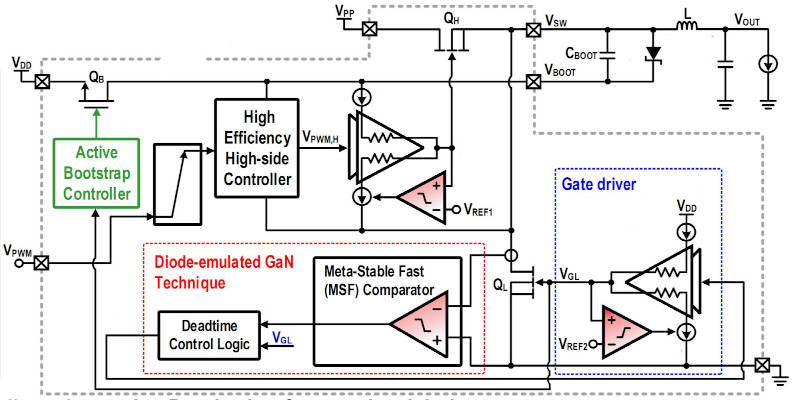
To retain control of gate voltage profiles at 50MHz the designers have implemented tight local feedback loops, creating a picosecond-realm comparator (dubbed ‘meta-stable fast’ – MSF – shaded red in the diagram) as the chip’s primary building block. To allow it to sense around its own negative supply, the comparators include a charge-pump which creates a more-negative bias voltage for the input stage.
Taking the low-side hemt driver as an example, current is driven into the gate at switch-on time, or vice versa.
The unusual part is the local feedback loop (simplified in the diagram) which monitors the gate voltage during its transitions using three MSF comparators which, through a logic block, have autonomous control of three current sources and three current sinks.
When the gate’s voltage profile deviates from the desired profile, during the Miller plateau for example, the local feedback loop automatically adds or subtracts current from the drive to push the voltage back on track.
As a design detail: the reference voltages for the three comparators are created by a totempole of gate-drain-shorted enhancement-mode hemts acting as constant-voltage devices, fed from the top by a depleation-mode constant current source.
In other parts of the circuit, diodes are created using gate-source-shorted e-hemts, using transitor geometry to match forward drop – these are ‘lateral field-effect rectifiers’.
There is more to the gate control
As the upper transistor of the half bridge is turned off, there needs to be a dead-band, however narrow, before the lower transistor is turned on to avoid cross conduction.
During this time, a diode is needed across the lower device to comutate the output inductor’s energy.
In a normal silicon mosfet, the parasitic anti-parallel diode can perform this task, and in GaN hemts there is diode-like reverse-conduction behaviour that will do something similar, but at a higher voltage drop than for silicon devices.
To improve efficiency, an additional control circuit in this design around the lower output transistor actively drives its gate to make it a better ‘diode’ during the dead-band before it is switched on fully.
Another efficiency-boosting feature is the third 650V hemt, which replaces the traditional diode in the booststrap circuit that powers the upper transistor driver. To get 50MHz operation, even this transistor has an actively-timed gate drive.
The finished chip has a 16.7mm2 footprint and, built into the converter, works across 48 to 400V with, using a 500nH output inductor, a peak efficiency of 95.4%.
Operating from 48V and delivering 4A, dead-band can be minimised to 120ps, or 140ps for 1A.
ISSCC 2022 Paper 14.1
A monolithic GaN-based driver and GaN power HEMT with diode-Emulated GaN technique for 50MHz operation and sub-0.2ns deadtime control
ISSCC 2022 is the 69th International Solid-State Circuits Conference, a conference which is arguably the world showcase for advances in on-chip circuit design and system-on-a-chip implementation. During the week-long conference, hundreds of selected and invited papers are presented, from the US, Asia and Europe.
The image is a modified form of Figure 14.1.1 in the ISSCC 2022 Digest of papers, with thanks to the IEEE, National Yang Ming Chiao Tung University and Realtek Semiconductor.


![W88 [Rủi Ro Khi Chơi Nổ Hũ: Lưu Ý Quan Trọng Nhất Cho Người Chơi]](https://theskil.com/wp-content/themes/rehub-theme/images/default/noimage_336_220.png)

